I think any start-up that is looking to build their first hardware product and doesn’t have all of the expertise in house, should consider working with Softeq. Because they bring experience from hundreds of projects to help make sure that as a start-up you don’t go through the mistakes that others have already made.

Jared Schrieber
President, Revolution Robotics
Case study
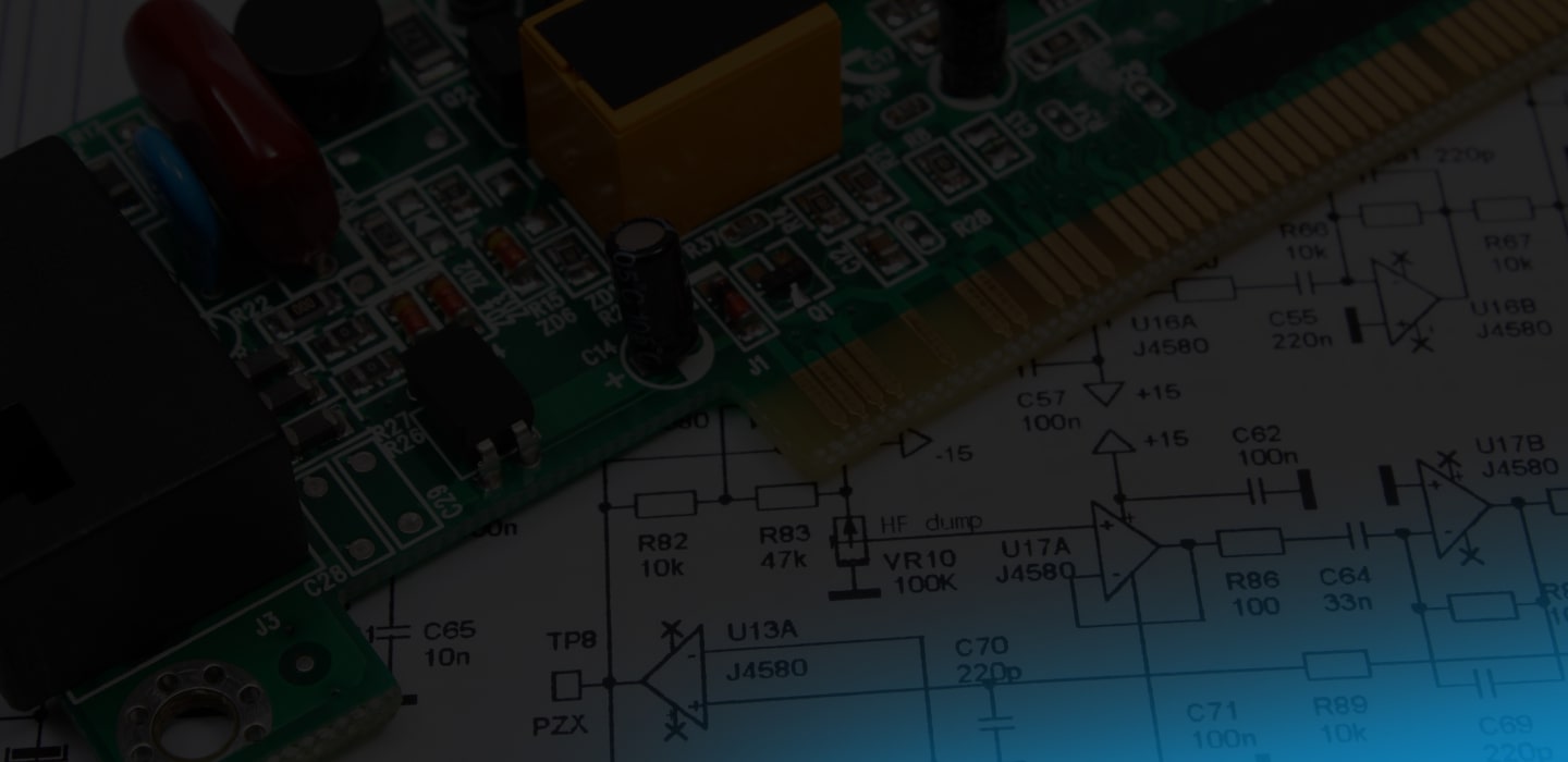
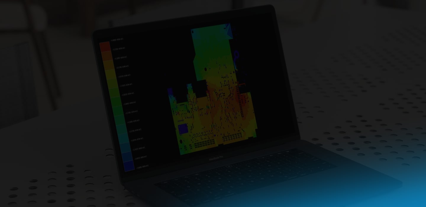
Electronic Kit for Revolution Robotics
The client addressed Softeq to develop an electronic kit that would allow users to assemble, program, and control robots via a smartphone.
Show Case Study